All posts by Chien Liu
Extracting Specific Contact Resistivity with a Benchmark Model
You can now add contact resistance to metal contacts using the Semiconductor Module. In this blog post, we’ll explore a benchmark model that takes advantage of this new functionality.
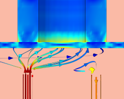
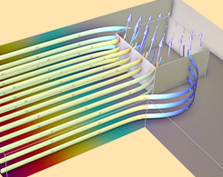
How to Simulate a Piezoelectric Micropump
Learn how to combine piezoelectric materials with fluid-structure interaction effects, use a velocity-dependent formula, and set up disconnected mesh between the solid and fluid domains.
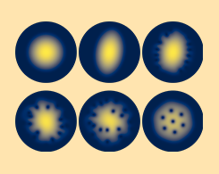
Simulating a Silicon Quantum Dot in a Uniform Magnetic Field
Solar cells, LEDs, displays, photodetectors, and quantum computing are all potential applications of quantum dots, an essential aspect in the field of nanotechnology.
k • p Method for Strained Wurtzite GaN Band Structure
Model a wide range of semiconductor systems, such as particles with spins and strained wurtzite crystals, using multicomponent wave function functionality in the Schrödinger Equation interface.
Model Vortex Lattice Formation in a Bose–Einstein Condensate
Bose–Einstein condensation can cause superfluidity, superconductivity, lasers, and trapped dilute cold atoms. When such systems are subjected to rotating perturbation, it forms a vortex lattice.
Three Semiconductor Device Models Using the Density-Gradient Theory
You can use the density-gradient theory to model semiconductor devices. Here are 3 examples: a Si inversion layer, Si nanowire MOSFET, and InSb p-channel FET.
Intro to Density-Gradient Theory for Semiconductor Device Simulation
The density-gradient theory is a computationally efficient way to include quantum confinement in the conventional drift-diffusion formulation commonly used for simulating semiconductor devices.
Simulating Radiation Effects in Semiconductor Devices
Analyzing radiation effects in semiconductor devices is an important capability for consumer electronics, medical imaging, nuclear engineering, aerospace, and a wide range of other industries.