
Graphene and other 2D materials are the focus of intense research and application interests due to their promising properties. In this blog post, we are going to use the example of a graphene-based THz metamaterial perfect absorber to demonstrate how to model 2D materials accurately and efficiently in high-frequency electromagnetics. The discussed techniques are equally applicable to modeling other thin layers, such as coatings on optical devices.
Introduction
Graphene is a material that consists of only a single layer of carbon atoms, which are arranged in a hexagonal lattice. Physicists have long postulated about the existence of a material with a single atomic layer. Decades ago, it was commonly believed that materials like graphene could not exist in nature because of the thermodynamic instability. In 2004, a team of physicists led by Konstantin Novoselov and Andre Geim from the University of Manchester experimentally demonstrated the existence of graphene for the first time. This discovery was considered so important and revolutionary that it was quickly awarded a Nobel Prize in 2010.
This material has been studied globally by physicists, material scientists, and engineers. Furthermore, more and more single-layer materials, such as hexagonal boron nitride, black phosphorus, tungsten disulphide, and so on, have been continuously discovered over the years. Nowadays, the demand for devices that contain these 2D materials continues to rise, hence the need for the multiphysics modeling of these materials.
Here, we are going to discuss different ways to model very thin materials like graphene in high-frequency electromagnetics. If you are interested in modeling optoelectronic or photonic devices with 2D materials or other thin layers, you will likely benefit from the techniques discussed below.
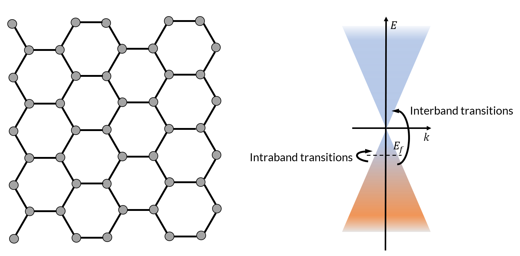
The image on the left shows the hexagonal lattice structure of graphene, where the grey circles represent carbon atoms. The image on the right shows the linear energy-momentum dispersion relation, which is often referred to as the Dirac cone, in graphene. Both the intraband and interband electronic transitions contribute to the conductivity of graphene.
Optical Conductivity of Graphene
Due to the linear energy-momentum dispersion, electrons in graphene behave as if they have no mass, which leads to very unique optical and electronic properties. The electromagnetic response of a graphene layer can be characterized by its 2D surface conductivity. Both the intraband and interband electronic transitions contribute to the total conductivity, i.e., \sigma_{2D} = \sigma_{2D}^{intra} + \sigma_{2D}^{inter}. Using the Kubo formulation, the intraband transition contribution is given by
where k_B is the Boltzmann constant, \hbar is the reduced Planck constant, T is the temperature, e is the electron charge, E_f is the Fermi energy, and \omega=2\pi f is the angular frequency. This contribution is dominant at low photon energies (the RF, microwave, and THz regimes). When the photon energy increases to infrared and optical frequencies, the electronic interband transitions kick in. The interband conductivity is given by
where the function H is
The COMSOL Multiphysics® software conveniently makes many physical constants available such as k_B, \hbar, and e; these constants can be used as k_B_const, hbar_const, and e_const, respectively. In addition, when using different quantities in different unit systems in one equation, the unit conversion is conveniently automatic. The integral in the interband conductivity can be calculated using the built-in integrate operator in COMSOL®. Notice that the upper limit of the integral is infinity. Numerically, we have to truncate it to a finite value. In this particular case, we found that 10^{16} rad/s yields the convergent result.
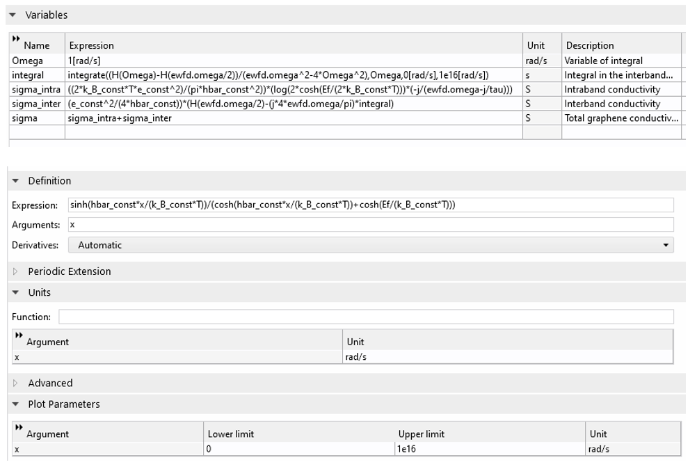
The defining variables and analytical function for calculating the conductivity of graphene. The usage of the built-in constants and operators greatly simplifies the implementation.
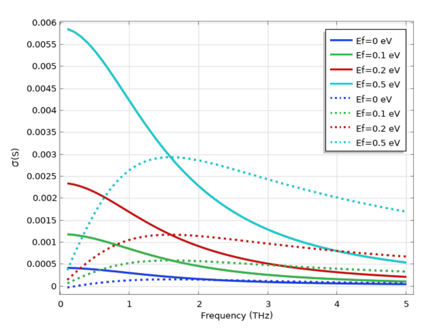
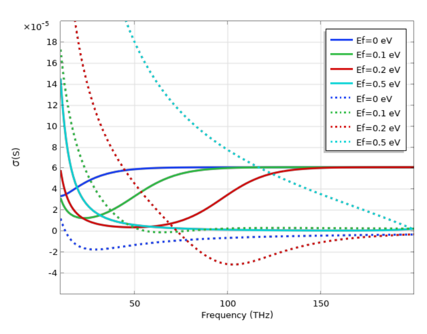
The calculated graphene surface conductivities for various Fermi energies in low frequency (THz) and high frequency (IR) are shown in the figures below. At low frequency, the conductivity follows a Drude-like response due to the dominant intraband transitions. At very high frequency, the conductivity approaches a universal value of \sigma_0=\frac{\pi e^2}{2h}\approx 6 \times 10^{-5} S, where h is the Planck constant. Here, we can also see the excellent tunability of graphene by changing the Fermi energy via electrical gating or chemical doping. This makes graphene a very desirable material in electronic and optoelectronic devices. Lastly, if we would like to treat graphene as a 3D slab, the 3D conductivity can be calculated from the 2D surface conductivity as \sigma_{3D} = \sigma_{2D}/d, where d is the (effective) thickness of graphene.
The graph on the left shows the graphene conductivity at the THz frequency range with different values of Fermi energy, where the intraband transition is the dominant effect. The graph on the right shows the graphene conductivity at the IR frequency range with different values of Fermi energy, where the contribution from interband transition becomes important. In both graphs, the solid curves represent the real part and the dashed curves represent the imaginary part of the conductivity.
Modeling Graphene in the RF and Wave Optics Modules
Now, how should we model graphene in an electromagnetic simulation? Due to its atomic thickness, explicitly modeling it as a 3D thin slab with the realistic thickness of ~0.34 nm is computationally intensive, and most likely unnecessary. Next, we are going to demonstrate three different approaches: using the Transition Boundary Condition, the Surface Current Density boundary condition, and a 3D slab of an effective thickness, respectively. We show that they all lead to practically identical results as far as the far-field spectrum goes. Note that the discussed techniques are general. They not only work for graphene, but any geometrically thin layers. As a concrete example, we are going to build a graphene-based THz metamaterial absorber, as proposed in Ref. 1.
In the absorber structure shown below, a fishnet pattern made of two graphene layers is embedded in a polymer background. A metal ground plane is inserted in the bottom to function as a reflector. The ground plane and the graphene effectively form a Fabry–Perot resonator. It’s easy to notice that the unit cell has two mirror symmetries. Therefore, a combination of the Perfect Electric Conductor and Perfect Magnetic Conductor boundary conditions can be used as symmetric planes so that only a quarter of the unit cell needs to be modeled. This is applicable when we consider normal incidence of the THz radiation, which is the case in this model.
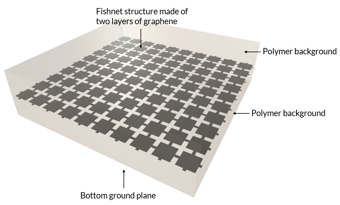
The graphene-based THz metamaterial absorber, which consists of a fishnet structure made of two layers of graphene embedded in a polymer background. The bottom of the model is a metallic ground plane.
In the RF Module and Wave Optics Module, the built-in Transition Boundary Condition is designed to model geometrically thin layers on interior boundaries. Physically, it represents a discontinuity in the tangential electric field due to the induced surface current densities
and
where Z_S = -\frac{j\omega\mu}{k}\frac{1}{tan(kd)}, Z_T = -\frac{j\omega\mu}{k}\frac{1}{sin(kd)}, and k=\omega\sqrt{\mu(\varepsilon+\frac{\sigma}{j\omega})}. The indices 1 and 2 refer to the two sides of the surface. By default, the Transition Boundary Condition assumes normal propagation in the thin layer, which is fulfilled in our model, while still assuming that the layer has a finite thickness. The (effective) thickness of graphene d can be set to any arbitrary small value, such as 1 nm, as long as the 3D conductivity is scaled correspondingly as \sigma_{3D} = \sigma_{2D}/d. Since there are two layers of graphene in this particular model, we will calculate the 3D conductivity as \sigma_{3D} = \sigma_{2D}/d while entering 2d as the thickness in the Transition Boundary Condition settings (please see the associated model, linked at the end of this blog post, for detail). As a side note, there is a distinctive difference between two separate graphene layers placed closely together and a bilayer graphene. When two separate graphene are layers placed closely together (such as in this model), the conductivity of each layer is unchanged. On the other hand, a bilayer graphene is two graphene layers that are bounded by van der Waals force. This bounding could significantly modify the properties of graphene depending on many factors, such as stacking order, twist angle, etc. That is, when modeling bilayer graphene or trilayer graphene, the conductivity needs to be calculated differently.
The simulated absorption spectra for our device at different Fermi energies are shown in the figure below. The result is consistent with Ref. 1. At 0.5 eV Fermi energy, a wide absorption band is present and the perfect absorption is obtained around 2.8 THz. The high absorption is caused by the Fabry–Perot resonator that is formed between the graphene and the bottom ground plane. When the resonance condition is met, high absorption in graphene is obtained. The absorption of this device can be actively tuned by, for example, adjusting the gate voltage on the graphene.
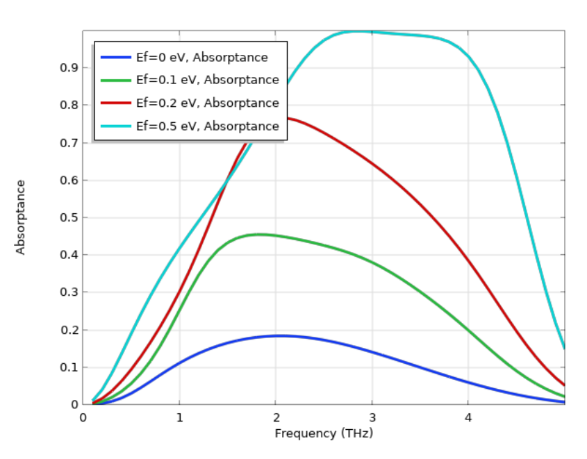
The absorptance spectra of the graphene-based metamaterial at various Fermi energies. The graphene is modeled using the Transition Boundary Condition.
Alternative to using the Transition Boundary Condition, we can directly model graphene using the Surface Current Density boundary condition, as briefly discussed in a previous blog post. This way, we truly treat graphene as a 2D layer without any thickness. Here, the current densities in the x and y directions are set to be J_x=\sigma_{2D}E_x and J_y=\sigma_{2D}E_y, respectively. Due to the thinness, we assume that there is no current flow in the z direction. This approach leads to a simulated absorption spectrum that is practically identical to that of the Transition Boundary Condition example, as shown in the figure below.
The techniques discussed earlier focus on modeling graphene by using specific boundary conditions, avoiding the explicit modeling of the graphene layer with 3D volume. This way, the simulation speed and RAM usage are greatly improved. In principle, we can model graphene in 3D as well. To make it as realistic as possible, one option would be to model graphene as a 3D slab with thickness 0.34 nm. However, in this particular model, we are concerned with THz radiation, where the wavelength is in the order of 100 μm. As long as the graphene thickness is much smaller than the wavelength, it makes no practical difference in terms of its optical response. Again, this is given that the 3D conductivity is scaled with the effective thickness appropriately. To demonstrate, we used an effective thickness of 100 nm in our simulation (the results can be seen in the scatter plot below). We can see that even though we used a seemly unrealistic thickness, the result is still mostly identical to the correct value. The ability to use a larger effective thickness is desirable because it helps mesh generation and avoids overmeshing. However, the requirements for CPU time and RAM are still significantly larger than in the previous methods.
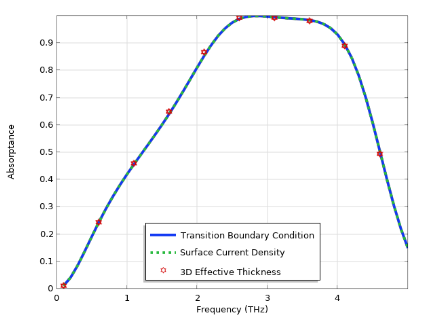
The absorptance spectra of the graphene-based metamaterial simulated using three different approaches: by using the Transition Boundary Condition, the Surface Current Density, and a 3D volume with effective thickness. The results are mostly identical, while the 3D volume takes significantly longer simulation time.
Final Thoughts
In conclusion, geometrically thin layers are ubiquitous in electromagnetic modeling. Besides 2D materials, common thin layers include antireflection coating on optical elements, conductive coating on electronic components, a thin metal layer on PCBs, and so on. The RF Module and Wave Optics Module provide built-in features like the Transition Boundary Condition and Surface Current Density to help reduce computational complexity when modeling geometrically thin layers. Making appropriate use of these features can greatly speed up your simulation while ensuring accuracy.
Next Step
Try the Graphene Metamaterial Perfect Absorber model yourself by clicking the button below, which will take you to the Application Gallery entry:
References
- A. Andryieuski and A. V. Lavrinenko, “Graphene metamaterials based tunable terahertz absorber: effective surface conductivity approach”, Opt. Express, vol. 21, pp. 9144–9155, 2013.



Comments (10)
Andy Sun
June 16, 2022Hello Tom,
Thanks for the great post, this is useful for graphene simulations.
I have a question here:
Can such boundary features be used in boundary mode analysis of 3D models? Especially when the graphene is parallel to the direction of a waveguide port.
Thanks in advance
Andy
Tom Chen
June 17, 2022 COMSOL EmployeeDear Andy,
We are glad that you found the blog post helpful.
That’s a great question. In terms of using the Transition Boundary Condition (TBC), the situation is a little complicated. The TBC will be recognized by the boundary mode analysis. However, the assumption of TBC is the wave propagation is normal to the thin layer. If your thin layer is parallel to the waveguide, it violates this assumption unless the conductivity of the layer is high. If the thin layer is perpendicular to the propagation direction, it should work fine as an approximation. Do keep in mind that what type of modes are propagating in your waveguide could also make a difference as the TBC assumes plane wave propagation inside. If you have a specific question regarding a model that you are working on, please feel free to contact our support team at https://www.comsol.com/support. We are more than happy to examine it with you.
Bests,
Tom
Muhammad Qamar
September 25, 2022Can you know how to make circular metamaterials
Tom Chen
September 26, 2022 COMSOL EmployeeHi Muhammad,
Could you be more specific about your application? By circular metamaterials, do you mean a metamaterial whose geometry is circular? If so, the model setup would be very similar to the tutorial model here but with some geometry changes.
Bests,
Tom
Aly Abdou
June 27, 2022Very nice blog post!
Muhammad Qamar
September 25, 2022Can you know how to make circular metamaterials
nidhi sharma
December 3, 2022Dear Sir ,
Please tell me that whether i can get “Graphene Metamaterial Perfect Absorber model” in version 5.3. Also i want PDF of all steps in the same version if you can provide then it will be a great help as i am a beginner in COMSOL.
Flávio Santos
May 10, 2023Hello dear Xinzhong (Tom) Chen.
I have recently started studying 2D graphene-based absorbers. Coming across your study here at Comsol, I saw that a conversion was made in the sign of the imaginary parameter “j” to “-j” in the Kubo equation, due to the phase conversion due to the reference it used, having used an analysis method different.
I would like to ask, how do I proceed with the 2D model, for the graphene permittivity equation? Since this phase conversion occurs in COMSOL. I thank the attention.
Telkom University
February 17, 2024Who were the physicists credited with experimentally demonstrating the existence of graphene for the first time, and what recognition did they receive for their work?
Regard Telkom University
Rida Alrahmanlokman Shahin
July 2, 2024Hi,
Thanks for the clear explanations.
I am wondering in the case of hundred of nanometer wavelength, in which way the model should be different, or it would be fundamentally similar?
Thanks!!