
Piezoelectricity finds use in a variety of engineering applications. They include transducers, inkjet printheads, adaptive optics, switching devices, cellphone components, and guitar pickups, to name a few. Today’s blog post will benefit both beginners and experts in piezoelectricity, as we highlight some of the fundamental elements of piezoelectric theory and basic simulations, along with a novel design for improving the range of motion for piezoelectric actuators.
The Mathematical Conventions of Piezoelectric Theory
Before we start discussing piezoelectric physics, let’s first review a couple of mathematical conventions. Piezoelectric materials have properties that allow strain to produce electric polarization and vice versa. The former is known as the direct piezoelectric effect, while the latter is referred to as the inverse piezoelectric effect. In mathematics, two forms of a set of matrix equations are conventionally used to describe these effects: the strain-charge form (also known as the d-form) and the stress-charge form (or the e-form). The two forms can be derived from each other by a transformation.
Note: The two forms are convertible, thus you can choose whichever option is preferred. In COMSOL Multiphysics, the strain-charge form is converted to the stress-charge form internally.
Here, we’ll choose the d-form, in which the relations are written as
\varepsilon & = s_E S + d^T \bf{E} \\
\bf{D} & = d\,S+\varepsilon_0 \varepsilon_{r} \bf{E},
where the field quantities \varepsilon, D, S, and \bf{E} are the strain, electric displacement, stress, and electric field, respectively.
The material parameters s_E, d, and \varepsilon_{r} are the compliance, coupling matrix, and relative permittivity, respectively. The superscript T stands for transpose. The first equation expresses the relation that the stress field and electric field produce strain. The second equation, meanwhile, shows the electric polarization generated by the stress field and electric field. The second term of the first equation accounts for the electric contribution to the strain.
In solid mechanics, we typically consider an imaginary, small differential volume to understand the force that is exerted on a volume. Let’s consider a volume where the surfaces are aligned to each axis of the global Cartesian coordinate system (xyz-axes).
There are six distinct quantities that describe the forces per unit area on the surface of the imaginary volume. Three of them are normal to each surface and are usually denoted by \sigma_{xx}, \sigma_{yy}, and \sigma_{zz}. The other three are parallel to each surface and are denoted by \tau_{yz}, \tau_{xz}, and \tau_{xy}. (\tau_{zy}, \tau_{zx}, and \tau_{yx} are omitted because of symmetry.)
The first index represents the normal vector of the surface under consideration. The second index indicates the direction of the force. For example, \sigma_{xx} is a force along the x-axis that is exerted on a yz-plane (a plane perpendicular to the x-axis); \tau_{yz} is a force along the z-axis on an xz-plane; and so on.
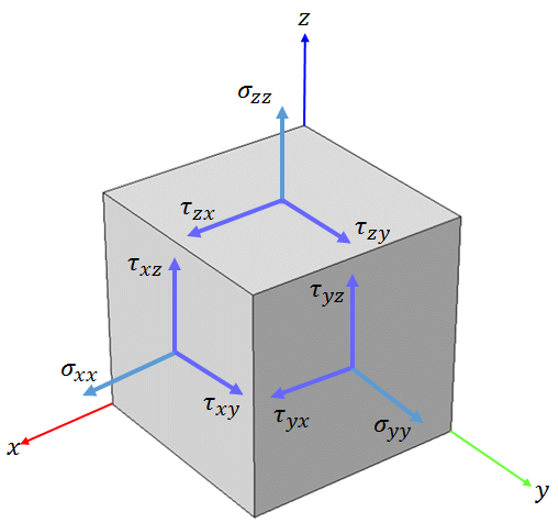
The force components in a small differential cubic volume.
These six quantities are often expressed as a column vector. In COMSOL Multiphysics, the order of the quantities has two conventions: one is the standard notation and the other is the Voigt notation. In COMSOL Multiphysics, it is important to make sure that the Voigt notation is used in the Piezoelectric Devices interface. (The standard notation is used by default in the Solid Mechanics interface.)
In the Voigt notation, the stress is written as a 6 x 1 column vector (special attention should be paid to the ordering of yz-, xz-, and xy– components):
\begin{array}{c}
\sigma_{xx} \\
\sigma_{yy} \\
\sigma_{zz} \\
\tau_{yz} \\
\tau_{xz} \\
\tau_{xy}
\end{array}
\right )
Similarly, the strain can be written as
\begin{array}{c}
\varepsilon_{xx} \\
\varepsilon_{yy} \\
\varepsilon_{zz} \\
2 \varepsilon_{yz} \\
2 \varepsilon_{xz} \\
2 \varepsilon_{xy}
\end{array}
\right )
In COMSOL Multiphysics, the coupling matrix d is defined by
=
\left (
\begin{array}{cccccc}
d_{xxx} & d_{xyy} & d_{xzz} & d_{xyz} & d_{xxz} & d_{xxy} \\
d_{yxx} & d_{yyy} & d_{yzz} & d_{yyz} & d_{yxz} & d_{yxy} \\
d_{zxx} & d_{zyy} & d_{zzz} & d_{zyz} & d_{zxz} & d_{zxy}
\end{array}
\right )
Here, the notation d_{xyz} reads as the coupling coefficient for the strain component \varepsilon_{yz} caused by the electric field component E_x. Now, in the Voigt notation, all of the subscripts are numeric with the rule:
As such, the coupling coefficient matrix is
=
\left (
\begin{array}{cccccc}
d_{11} & d_{12} & d_{13} & d_{14} & d_{15} & d_{16} \\
d_{21} & d_{22} & d_{23} & d_{24} & d_{25} & d_{26} \\
d_{31} & d_{32} & d_{33} & d_{34} & d_{35} & d_{36}
\end{array}
\right )
Thus, the electric contribution can be rewritten as
\begin{array}{c}
\varepsilon_1 \\
\varepsilon_2 \\
\varepsilon_3 \\
\varepsilon_4 \\
\varepsilon_5 \\
\varepsilon_6
\end{array}
\right )
=
\left (
\begin{array}{ccc}
d_{11} & d_{21} & d_{31} \\
d_{12} & d_{22} & d_{32} \\
d_{13} & d_{23} & d_{33} \\
d_{14} & d_{24} & d_{34} \\
d_{15} & d_{25} & d_{35} \\
d_{16} & d_{26} & d_{36}
\end{array}
\right )
\left (
\begin{array}{c}
E_1 \\
E_2 \\
E_3
\end{array}
\right ).
In the view of the material property settings in COMSOL Multiphysics, the matrix d is flattened into a 1 x 18 row vector to be concise. It then looks like the following:
We always have the option to view the expression in the matrix form. We can do so by clicking on the Edit button in the “Output properties” section, as shown below:
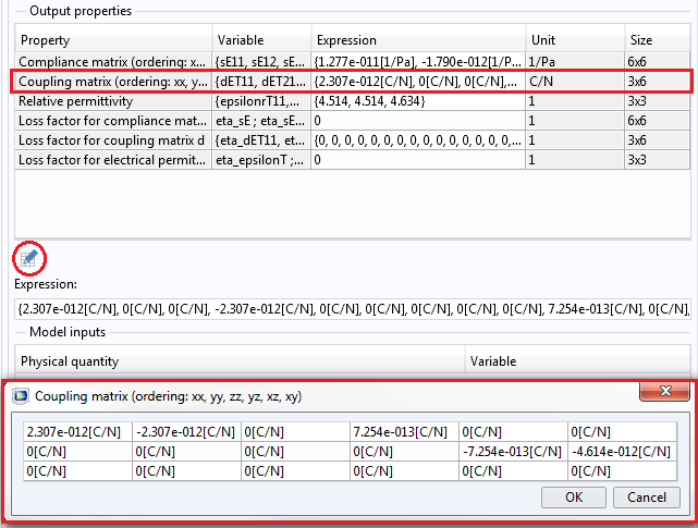
A screenshot of the COMSOL Desktop shows the d coefficients in a matrix form.
Basic Piezoelectric Simulations
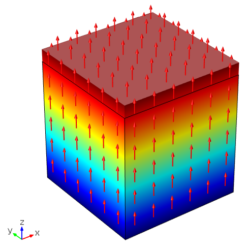
Now that we’ve reviewed some of the basics of piezoelectric theory, let’s turn our attention to performing simulations. Here, we’ll enter a nonzero number only in d_{33}. This means that the piezoelectric material makes a normal force along the z-axis by the z-component of the electric field E_z. We also assume that the bottom surface is mechanically fixed.
The results shown below are obtained, with the surface color representing the total displacement and the arrows indicating the electric field. The contribution of the electric field to the strain is given by E_3 d_{33}. The black outline indicates the initially undeformed shape. As indicated by the plot, the volume is stretched in the z-axis direction.
An example of the d coefficients with the only nonzero in d_{33}. Under an electric field along the z-axis, the volume stretches along the z-axis.
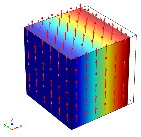
Keeping the same electric field, we’ll now enter a negative coefficient only in d_{31}. With the yz-plane mechanically fixed, the volume shrinks in the x-axis direction.
An example of the d coefficients with the only nonzero negative in d_{31}. Under an electric field along the z-axis, the volume shrinks in the x-axis.
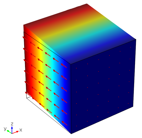
The last preliminary example shows a shear force, with a nonzero number entered only in d_{24}. The xz-plane is mechanically fixed and an electric field is applied along the y-axis.
An example of the d coefficients with the only nonzero in d_{24}. Under an electric field along the y-axis, the volume experiences a shear along the yz-plane.
Building on these basic elements, we’ll now introduce you to a helpful trick for designing piezoelectric actuators — a piezoelec”trick”, if you will.
Improving the Range of Motion in Piezoelectric Actuators: A Novel Design
Simulating a Piezoelectric Cantilever, a Simple MEMS Device
On its own, a piece of piezoelectric material is not a MEMS device. To become such a device, it must be attached to other elastic materials. Cantilevers are one of the simplest MEMS examples, and there are two different piezoelectric types. The first is the unimorph type, which is typically a sheet made by attaching a single layer of piezoelectric material to an elastic material. The other is the bimorph type, which is composed of two piezoelectric layers and other elastic materials. The materials used for attachment can be almost anything, as long as it is possible to put an electrode layer on their surface. Here, for simplicity, we will consider a unimorph type of MEMS device.
It is worth mentioning that all of the piezoelectric material properties provided by COMSOL Multiphysics are assumed to be poled in the z-axis of the local coordinate system. If the material is poled along another direction, you need to define a coordinate system so that its third direction is aligned with the poling direction.
COMSOL Multiphysics provides convenient functionalities to set up local coordinate systems. To learn more, you can refer to page 106 in the Structural Mechanics Module Users Guide. You can also consult the Piezoelectric Shear-Actuated Beam and Thickness Shear Mode Quartz Oscillator models, found in the Application Libraries under the Piezoelectric Devices interface in the MEMS Module and also on our website.
Under the assumption referenced above, we model a unimorph piezoelectric cantilever that is fixed at one end. From the Material Libraries, we select barium titanate (BaTiO3) as a piezoelectric material and silica (SiO2) as the substrate.
The principle of the MEMS device is simple. An electric field is applied in the z-direction, causing shrinkage in the x-direction due to d_{31} (=-7.8e-11 [C/N]). Note that the elastic properties of the electrode are not modeled here. To achieve the z-directional electric fields, an electric potential is applied on one side of the barium titanate, while the other side is grounded. With the left end mechanically fixed, the MEMS cantilever moves about 9 um at the free end. As the top material (BaTiO3) shrinks, it pulls the bottom material (SiO2), causing the entire device to bend in the upward direction.
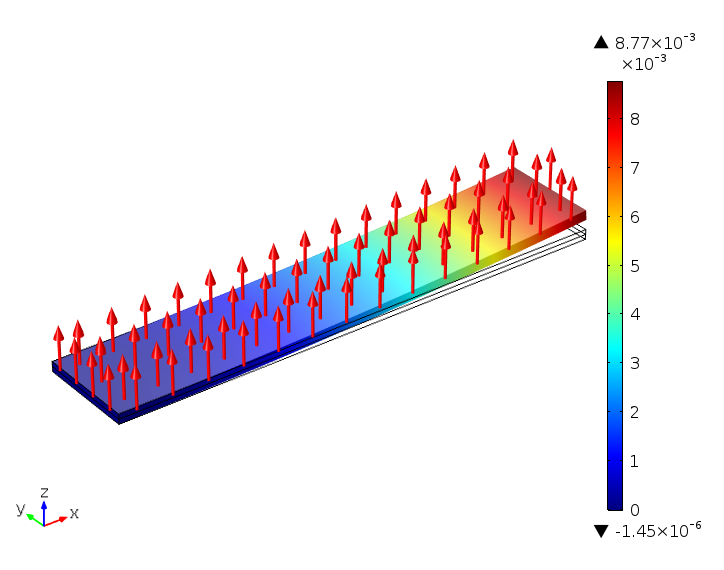
A unimorph cantilever with a fixed end shows the total displacement.
But what if we have to fix both ends of the device for some reason — perhaps mechanical ruggedness? The result is obvious: There is almost no displacement, as the top material cannot shrink along the x-axis at all. More accurately, the only displacement is due to the d_{32} effect, which is not intended.
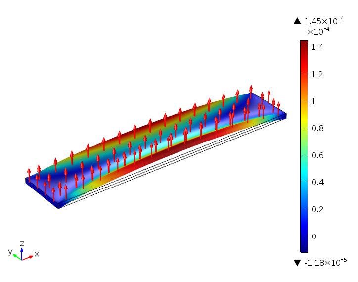
A unimorph cantilever with both ends fixed shows almost no displacement.
It is, however, possible to overturn such a situation. We can do so by modifying the piezoelectric device with a little “trick”. As the resulting plot below shows, the displacement is now back to the same order of magnitude. If you look at the electric field directions, what we have done to obtain this result is apparent. The electric field is reversed in the center part of the beam. You can perform the trick by patterning the electrode into three parts: a center and two sides, grounding them alternately and applying a voltage alternately in the opposite order as in the first of the next two figures.
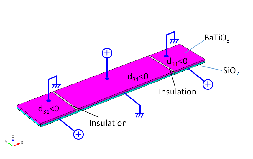
Material and voltage configurations in a unimorph cantilever with both ends fixed under alternate electric fields.
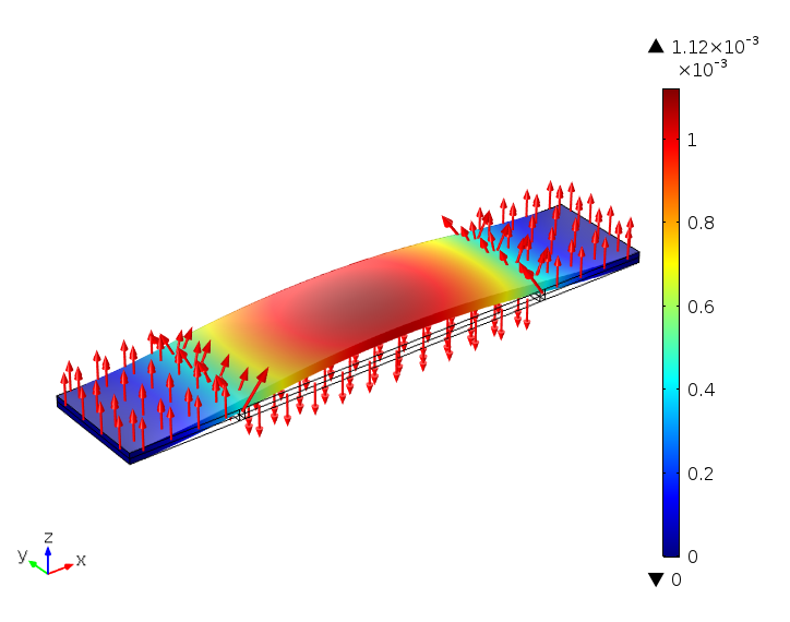
A unimorph cantilever with both ends fixed. Applying alternate electric fields improves the total displacement.
Let’s look at another example. It may seem a bit mysterious at first sight, as the entire electric field is aligned in the same direction. Still, we have the same performance as the previous result without alternating the electric field. We instead alternate the piezoelectric material, splitting it into three parts (again, a center and two sides) and flipping the center part.
With regards to simulation, this can be done either by using different local coordinate systems or, in a simple case like this, by changing the sign of the coupling coefficient, d_{31}. In practice, we can really split the piezoelectric material up and put the flipped part in the center. An easier and more practical approach is to pattern the electrode in the same manner as the previous example, but pole the center part in the opposite direction. There is no need to split the material in such a situation.
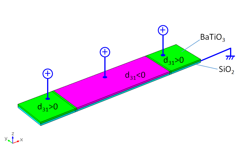
For the unimorph cantilever with both ends fixed, alternate material and voltage configurations.
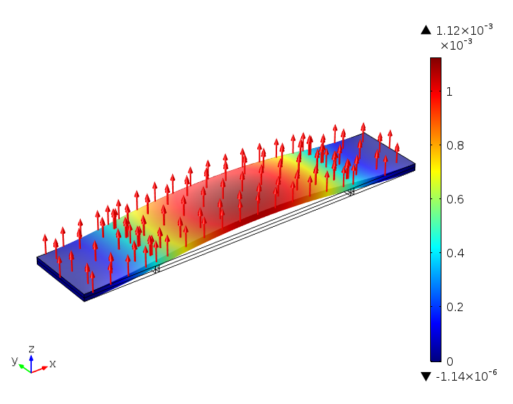
For the unimorph cantilever with both ends fixed, alternating the poling direction also improves the total displacement.
Simulating a Piezoelectric Membrane MEMS Device
Our last example is particularly interesting. Without the use of a trick, we would really have no displacement, since the entire perimeter is fixed and, as such, there is no room for any d_{3*} component to play a role. Applying the same trick from the previous examples, the entire-perimeter-fixed membrane can have a tremendous displacement. The simulation shown here can be used as a MEMS device that compensates for, to name an example, optical aberration (particularly spherical and astigmatism).
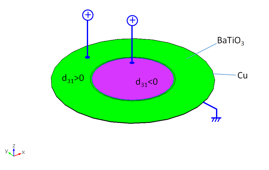
Alternate material and voltage configurations in a membrane MEMS device with the entire perimeter fixed.
A membrane MEMS device with the entire perimeter fixed. Applying an alternate electric field or poling direction improves the total displacement.
From the Basics to a Helpful Design Trick
We have reviewed some of the fundamental mathematics and conventions that are necessary when simulating piezoelectric materials. Further, we have walked you through the steps of performing basic simulations, then diving into more interesting applications using our piezoelec”trick”.
When it comes to the trick, the secret to significantly improving the displacement is the “inflection zone”, which is created by alternating the electric field or the material property. (Refer to US Patent 7,369,482 for more details and other examples.) The local coordinate system functionalities of COMSOL Multiphysics make it very easy to set up a simulation for such systems with alternating material orientations.
If you enjoyed today’s blog post, be sure to check out some other related blog posts that might spark your interest:






Comments (11)
Ivar Kjelberg
February 17, 2016Hi
Thanks for a nice and well documented Blog, it also helps for the coherence of the PZT tensor representation.
Concerning the engineering trick applied to increase the displacements, it’s indeed nice and works for the displacements, but you do not show the stresses! nor the related forces obtained.
To increase the displacement one must concentrate the stresses highly in the electrode interstice regions, this must be carefully estimated as its a clear failure mode case 🙂
So you talk only about half the engineering issue for such an enhanced PZT displacement finger.
Sincerely
Ivar
Yosuke Mizuyama
February 22, 2016 COMSOL EmployeeDear Ivar,
Thank you for your message. It is fair to say that the stresses here will be reasonable, but this blog is not meant to address all of the various engineering issues associated with piezoelectric device design. For your information, the stresses are actually moderate around the interstice regions. It has never broken from that part. It has broken from another part, instead. The key is, as written in this blog, to make the device shape concave on the fixed edge sides and convex in the center by giving inflection zones. Of course, you are certainly welcome to build a model of this device and verify the stresses and failure criterion if you would like.
Best regards,
Yosuke
Ivar Kjelberg
February 25, 2016Hi Yosuke
PLS do not see any negative critic about your blog: it’s great, and the “trick” very nice. I mainly wanted to stress that with COMSOL you can do also more, such as see in detail the stress buildup, the local electric field across the electrode separation … and all under the same tool.
OK all COMSOL users know that, but for me, these Blog pages are also read by “want to become COMSOL users” that might not be aware of it, as there are for me no other FEM tools on then market with all these different physics possibilities 🙂
Sincerely
Ivar
Yosuke Mizuyama
February 25, 2016 COMSOL EmployeeHi Ivar,
Yes, I agree. We can show that COMSOL can do more. Maybe I can write another one for the same series in the future.
Thank you for your comment.
Best regards,
Yosuke
Rajesh kumar
February 8, 2019Hi,
Could you show the that COMSOL simulation procedure. I am try to simulate this module, but this not compute or else give the link for simulation file.
Thanks and Regards,
Rajesh
Yosuke Mizuyama
February 8, 2019 COMSOL EmployeeHi Rajesh,
Thank you for reading my blog. Unfortunately, it’s too complicated to explain the procedure here. I will try to publish this model soon. Otherwise please send a request to support@comsol.com.
Best regards,
Yosuke
Akash Kumar
December 24, 2019Hi
Thanks for the nice documentation and explanation. the explanation is very well mannered.
And again I thank for this blog.
Shin Jun Hyuk
January 28, 2020Hi
Thanks for your explanation.
I am student interested in piezoelectric actuator and i just saw your blog.
Is it possible to show polarization direction as well?
I just started studying COMSOL and i would like to know the step by step process of your simulation.
So..Would you mind if I get .mph file that you solved?
Sincerely,
Shin Jun Hyuk
Yosuke Mizuyama
January 29, 2020 COMSOL EmployeeHi Akash and Shin Jun Hyuk,
Thank you for reading my blog and thank you for your patience.
We are trying to publish the model. I hope it will come out soon.
Best regards,
Yosuke
Ameya Abhay Kale
May 18, 2020Thank you for this post, Yosuke! Eagerly waiting for the model file to simulate this properly myself and try playing with other parameters!
Mirhan Özdemir
November 13, 2020Sir thank you for your explanations, but it is still hard to understant the concept because of ‘trick’ that u mentioned. If it is possible would you share “Simulating a Piezoelectric Membrane MEMS Device” model so that we can go through each step. Thank you.