
The Coplanar Waveguide (CPW) is commonly used in microwave circuits. COMSOL Multiphysics, with the RF Module, makes it easy to compute the impedance, fields, losses, and other operating parameters needed when designing a CPW.
Grounded Coplanar Waveguide Design in 2D
Two typical Coplanar Waveguides are diagrammed in cross section below. A dielectric substrate has metal layers patterned on top of it. When a metal layer is also present underneath the substrate, it is known as a Grounded Coplanar Waveguide. This metal layer is typically connected with vias to the metal layers above the dielectric. Although these metal layers are often called grounds, keep in mind that there is a current flowing through these metal layers, hence the surfaces are not at a constant potential. We will focus on the Grounded CPW case.

The CPW is characterized by the metal trace layer thickness, t, the center conductor width, w, the gap, g, between center and side conductors, and finally the dielectric substrate thickness, h, for the grounded case.
One of the first quantities you should calculate, prior to any modeling, is the skin depth:
![]()
Considering copper, for example, used in a device operating at a frequency of 1GHz, the relative permeability and permittivity are unity, and the conductivity is 6×10⁷ S/m, for a skin depth of 2.05 microns. This means that the electric fields and currents fall off as: ![]() , where
, where ![]() is the distance into the metal. The skin depth and the thickness of the metal layers will govern what kind of analysis you will need to do. If the skin depth and trace thickness are comparable, then it is necessary to include the metal domains themselves in the COMSOL model. On the other hand, if the skin depth is much smaller than the thickness, by at least a factor of ten (
is the distance into the metal. The skin depth and the thickness of the metal layers will govern what kind of analysis you will need to do. If the skin depth and trace thickness are comparable, then it is necessary to include the metal domains themselves in the COMSOL model. On the other hand, if the skin depth is much smaller than the thickness, by at least a factor of ten (![]() ), then the fields on one side of the metal layer do not significantly affect the fields on the other side. In such cases, it is not necessary to model the interior of the metal layers; they can be considered boundaries of the modeling domain.
), then the fields on one side of the metal layer do not significantly affect the fields on the other side. In such cases, it is not necessary to model the interior of the metal layers; they can be considered boundaries of the modeling domain.
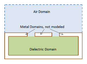
Additionally, if the thickness, t, of the metal layers is small enough, such that the thickness becomes negligible to the results, it becomes possible to model the metal traces as Perfect Electric Conductor (PEC) boundary conditions, as shown in the diagram below of the simplest model of a CPW. The air region above the CPW can be truncated by either a PEC boundary condition, representing the metallic packaging, or a Perfect Magnetic Conductor (PMC) boundary condition, representing a surface along which no current can flow.
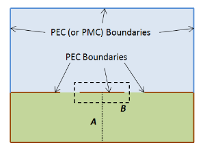
Such a model can be set up and solved in the RF Module, using the 2D Mode Analysis Study Type; computing the impedance, Z=V/I; computing the voltage, V, by taking the path integral of the electric field along an arbitrary line between the conductors, here marked A; and computing the current, I, by taking the integral of the magnetic field along an arbitrary path, marked B, encircling the center conductor. The Finding the Impedance of a Coaxial Cable model provides a similar example that goes into more details about setting up such models.
Three Techniques for Creating a 3D Model of a Coplanar Waveguide
Now, such 2D models can quickly compute the impedance of the CPW, and give you an idea of the relative field magnitudes in the cross section. However, we are typically more interested in devices that have some variations to their structure that require a full 3D model. This raises the question of how to excite the 3D Coplanar Waveguide model. Several different techniques are possible, but we will start by considering a CPW that can be modeled using PEC faces, where the trace thickness, t, can be considered negligible.
1. Adding Rectangular Faces to the Model
One approach, diagrammed below, is to add several rectangular faces to the model, either normal or parallel to the plane of the CPW, that represent a probe tip. These PEC faces act as a bridge between the two side conductors. A Lumped Port excitation is then applied to another rectangular face between the bridge and the center conductor. This Lumped Port applies a voltage difference between adjacent PEC faces (note: the directions of the arrows in the figure are arbitrary; they are merely meant to show that there is an applied, sinusoidally time-varying, current flowing in the direction of the arrows).

This approach is quite straightforward, requiring only a minor modification of the model. To see an example of a CPW model excited using this technique, check out the SMA Connector on a Grounded Coplanar Waveguide model in the Model Gallery.
2. Less Modification with Two Lumped Ports
Now, the above approach does require adding some extra structures to the model, so you may consider an approach that requires even less modification, as shown in the figure below. By adding two Lumped Ports on either side of the center conductor, the CPW can also be excited. The only difficulty with this approach is that it will require you to manually set; the Port Number to be the same in both Lumped Port features; the dimensions; and, most importantly, the direction. The direction of the Lumped Ports must be set so that they are either both pointing towards, or both pointing away from, the center conductor.
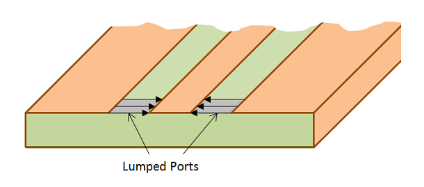
This approach introduces less extra structure into the model, but does require having two port features — that have to be manually set and point in the correct directions.
3. Mimicking a Two-point Probe
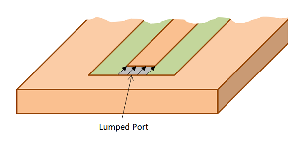
It is also possible to extend the layout of the CPW and extend the side PEC planes to surround the center PEC strip, and then introduce an additional rectangle for the Lumped Port, mimicking a two-point probe, as shown here:
Comments on the Approaches for Exciting a CPW
There are certainly other ways in which a CPW can be excited, but the above three approaches are the most common. The differences, in terms of the solutions, should be small between all three approaches, but it is worth noting that all of these are meant to approximate an excitation, and the fields in the immediate vicinity of the Lumped Port will not be physically realistic. This is a local effect, the fields away from the excitation and quantities such as the computed impedance will be more accurate.
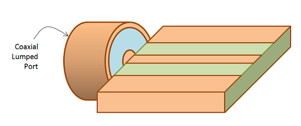
For highest fidelity, it is possible to explicitly model the coupling to a coaxial waveguide, which is modeled with full details, as shown in the figure above. For a similar example that exemplifies this technique, please see the Wilkinson Power Divider model.
All of the above techniques can be generalized to the case when the thickness of the metal traces of the CPW is significant, or to the case when the metal layer must be explicitly included in the model, rather than approximated via a boundary condition. Other excitation strategies are certainly possible, but these represent the most common methods. Knowing these techniques will give you the confidence to approach your modeling and design of coplanar waveguides using COMSOL Multiphysics and the RF Module.


Comments (16)
Bojian Xu
September 5, 2014The link of “Coplanar Waveguide (CPW) Bandpass Filter” seems to be disabled.
Fanny Griesmer
September 5, 2014 COMSOL EmployeeHi Bojian,
Thank you for bringing this to our attention. We have replaced the example with an SMA Connector on a Grounded Coplanar Waveguide model and updated the link.
Niklas Liebing
February 27, 2015Thanks for the nice introduction. Is there any dependency on the dimensions of the air bridge (e.g. border width or height of the air bride) in section 2 or the dimensions (along the wave guide) of the lumped port in section 3.
Walter Frei
February 27, 2015 COMSOL EmployeeHi Niklas,
There is a weak dependency, yes. You’ll want to keep these faces relatively small. If you make them too large you will introduce additional capacitance into the model.
Runyu Liu
February 14, 2016Hi Walter,
Can we have a 5.1 version of the CPW bandpass filter?
Now I need some help on setting up the lumped port for my CPW based filters. Really want to look at the example, but only have 5.1 COMSOL installed.
Thanks,
Runyu
Walter Frei
February 16, 2016 COMSOL EmployeeDear Runyu,
If the model you are asking about is:
http://www.comsol.com/model/coplanar-waveguide-bandpass-filter-12099
this model is available in version 5.2.
We do always encourage our on-subscription customers to upgrade to the latest version of the software, and to renew their subscriptions as this will keep you up to date with all the latest software features and example models.
Best Regards,
xin zhou
January 28, 2018Dear Walter Frei,
Thanks a lot for your blog. you have showed three Techniques for Creating a 3D Model of a Coplanar Waveguide. But if i want to simulate a LC looped resonator in 2D mode, how can I set the lumped port ? For example, I want to simple simulate a CPW transmission line with structure of center line 10 um and with 5 um gap to each two ground plane. There is no ‘multi elements’ can be chosen in Lumped Ports, like in 3D. How can i solve this problem ?
Best wishes
Walter Frei
January 29, 2018 COMSOL EmployeeDear Xin,
coplanar waveguide circuit structures, such as a looped resonator, are inherently 3D, so you do have to model in 3D to get the full-wave solution.
xin zhou
January 29, 2018Dear Frei,
thanks for your reply. Simulation looped resonator in 3D model becomes difficult when we consider multilayer structure. For example, if the whole substrate contains a sub-box 300 um thickness and an oxide layer 0.1 um, meshing looped resonator on this kind multi-layer substrates will be very difficulty. Although thin oxide layer (comparing to thickness of substrate) on top of substrate will not influence CPW mode so much, does comsol has some tricks to solve this meshing problem ?
家辉 陈
May 20, 2018Hi Walter,the mode field and electric dispacement of microwave transmitting in coplanar waveguide in 2D structure are what I need, I have read Finding the Impedance of a Coaxial Cable,but I found some difference between coplanar waveguide and coxial cable:to compute the impedance,I couldn’t find the path mentioned in the blog while computing the voltage and current,could you show more details about modeling the coplanar waveguide?Thanks.
Yongqi Shi
July 14, 2020Dear Walter, thanks for your article. In the last paragraph, you mentioned that all the three techniques can be generalized to the case that the metal trace thickness is modeled. This is the case which I’m working at. I use multi uniform lumped ports like what you wrote in figure of the Sec 2, while my metal thickness is 20um, and I also set the very narrow vertical boundaries (where the lumped ports are put between) to be PEC. While when I’m performing the solver, it also alarms that the lumped ports should be put between two conductive boundaries. What could be the reason for that? How can generalize to this case? I’m working at 21 GHz and the sizes of the lumped ports are 388um*130um.
Jagmohan Singh
July 4, 2021Dear Walter,
I want to find the S-parameters of a CPW at different temperature such that the temperature will modify the material properties. Can you please suggest how can I do that .
Thanks,
Jagmohan
Semih Cakmakyapan
June 16, 2022I’m also interested in this problem. I’d appreciate it if you could guide me with this as well.
Thanks,
Walter Frei
June 16, 2022 COMSOL EmployeeHello,
Regarding modeling of RF devices heating up during operation, good places to start are:
https://www.comsol.com/model/rf-heating-6078
https://www.comsol.com/model/thermo-structural-effects-on-a-cavity-filter-89071
Walter Frei
February 8, 2023 COMSOL EmployeeFor a more complete overview of this topic, we now also have this resource:
https://www.comsol.com/support/learning-center/article/Modeling-TEM-and-Quasi-TEM-Transmission-Lines-49931
Ananya Susan Cherian
January 24, 2024can i get the coplanar waveguide resonator file in 5.6 version as well